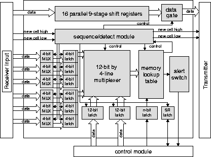
The Analysis Module admits a new cell into a 16-bit shift register, word by word from the receiver. In parallel, as components of the VPI/VCI pair belonging to the cell in transit are received from the Receiver (contained in the cell header, consisting of the first five bytes of data) they will also be copied into six four-bit latches.
Once all 24 bits of the VPI/VCI pair associated with the cell in transit have been captured in these four-bit latches, the 24 bits of output from them will be presented to the memory lookup module in two 12-bit words, with one word being presented at a time. The control to present these two 12-bit words will be performed by a 12-bit by 4-input multiplexor.
The two words that are presented to the memory lookup module will be interpreted by this module as an address that is uses to perform the actual analysis of the cell's validity. Depending on the version of the Analysis Module to be implemented, this function will change. Primarily, the memory lookup module will verify if the cell belongs to a connection that does indeed pass through the switch and port from which it originated. Optionally, the module will also verify if the network connection along which the cell in question is traveling has is within the envelope defined by the maximum and minimum traffic bounding function for that connection at that output port.
This result will be used by the sequence/detect module to determine if the cell is valid or not. If the cell is valid, it will enable the output from the last set of latches in the 16-bit shift register to be sent out to the transmitter. If the cell is not valid, the sequence/detect module will suppress output of the cell from the shift register to the transmitter by simply presenting null data (all zero bits) to the input state of the Receiver. In this case, the sequence/detect module will also trigger the interrupt logic in the Control Module. The Control Module will then know that an invalid cell has been detected and will perform the necessary operations to read the VPI/VCI pair of the offending cell from the outputs of the six 4-bit latches, which have been storing this information throughout the entire process.
All the devices used in this circuit are currently feasible in TTL and HC logic families. In addition, a number of tri-state buffers are implicitly used in this design to allow the Control Module to select between the data inputs and outputs of the different Analysis Modules to which it is attached. The interconnection of the functional blocks of the Analysis Module is shown in Figure 4.
The sequence/detect module is a simple sequential state machine with external decode logic. It controls all the inputs and outputs required to perform the functions just described. This state machine is designed using the same type of edge triggered D-type latches and combinatorial logic used to construct the other component blocks of the Analysis Module.
The reasoning behind the design of the Analysis Module was to be able to take advantage of the large number of operations that can be performed in parallel in order to reduce the number of clock cycles necessary for the device to perform its function.
The effect on the performance of the physical communication link passing through this device will be that any cell in transit will be delayed by the amount of time necessary to read in the cell's header and perform the lookup of the VPI/VCI pair contained in these five bytes in the memory lookup module. This means that the controlling factor of the transmission delay a cell will experience in every security device through which it passes will be the sum of these two periods of time, in addition to delays incurred due to link-level synchronization at receivers and transmitters.
The Control Module's logic will be triggered within less than one cell transmit time if the transiting cell is found to be invalid (nine clock cycles, to be precise). This means that the Control Module will know about the violation in less than one cell time and can begin sending data bout the violation to its supervisory control interface within less than one cell time.