
All three types of memory -- SDR, DDR, and RDRAM -- are physically organized as modules, composed of multiple devices, each of which is an individually-packaged integrated circuit. The traditional SDR and DDR architectures use wide (64 or 72-bits) data buses at relatively low clock rates (typically, 100 or 133 MHz), and require all devices on the same module to operate in parallel.
In comparison, Rambus DRAM technology [33] transfers data on a narrower 16-bit data channel, operating at twice the clock rate of 400 Mhz, to provide an extremely high throughput to better match the bandwidth needs of modern microprocessors. By using a narrow data bus, only a single device in the module needs to be actively transferring data at a time. This results in a lower power dissipation than for SDR or DDR, where all the devices in the module are activated in parallel to fill the wider bus. Furthermore, since they are not accessed in parallel, the devices in an RDRAM module can be in different power states, giving us a device-granular control in power management, in contrast to the traditional SDRAM architectures which can only provide module-granular control. Due to this finer-grained level of control, we will primarily focus on Rambus memory, although our approach is also applicable to SDR and DDR architectures, as we will show in Section 5.6.
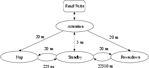 |
There are four power levels of interest defined in the RDRAM specification, listed in decreasing order by power dissipation: Attention, Standby, Nap, and Powerdown. Devices are put into lower power levels by disabling the auxiliary subcomponents as discussed previously. For example, while in Attention mode, the self-refresh circuitry and the row/column decoders are active, and the internal clock is kept in-sync with the external clock generator, whereas in Powerdown mode, only the self-refresh circuitry is active to prevent data loss. The details of these power levels and the power dissipation of each are shown in Table 1. However, since read or write operations can only be performed on a memory device when it is in Attention mode, a resynchronization cost is incurred to return a device to Attention mode if it is in any lower power states. The possible state transitions and the corresponding resynchronization costs are shown in Figure 3.
Current RDRAM memory controllers already have a rudimentary form of power-saving policy built-in. Instead of having all devices in Attention mode, the memory controller puts all devices except for the one currently being accessed in Standby mode. Due to the small resynchronization time and the large power difference between Standby and Attention modes, power is significantly reduced with almost no performance loss. Using PAVM, we will show that an additional 59-94% power reduction can be achieved by exploiting the Nap mode with only a negligible performance overhead. Due to the large difference in resynchronization time and the small difference in power between Powerdown and Nap modes, Powerdown mode is rarely more suitable for use in dynamic power management than Nap mode, as is verified in [9]. So, in this paper, we do not consider Powerdown mode.