| ||||||||||||||||||||||||||||||||||||||||||||||||||||
|
USENIX Technical Program - Paper - Smartcard 99
[Technical Program]
Feasibility of Smart Cards in Silicon-On-Insulator (SOI) Technology
Amaury Nève, Denis Flandre and Jean-Jacques Quisquater Université Catholique de Louvain Microelectronics Laboratory Place du Levant 3 B-1348 Louvain-la-Neuve, Belgium
Abstract Applications involving smart cards have rapidly emerged since a few years. Up to now, chips are realized in conventional bulk technology. But as the need for performance rises, alternative technologies must be investigated. In this paper we study the feasibility of realizing the blocks for a smart card chip in Silicon-On-Insulator (SOI) technology. For most of the circuit blocks, SOI realization already exists and may be adapted for this application. However, we identified two circuits never fabricated in SOI: a charge pump and the random number generator. The charge pump has been realized in SOI and tested. A random signal source has also been realized. The circuit to create random bits, based on this source, is exposed.
1. Introduction Applications involving smart cards have experienced a huge rise in recent years [1], [2], [3]. From simple memory cards at the origin, they evolved towards complex system-on-chip cards integrating memories, CPU, arithmetic co-processor and control logic. This opened new opportunities: smart cards can of course retain a huge amount of information compared to the magnetic strip cards, but they can also manage this information much more securely, using authentication and user identification procedures. The main improvement is the possibility to process the information directly on the card. Chips for smart cards follow the general trends in microelectronics [1]: towards small dimensions and towards low-power, low-voltage circuits. The performances required from the electronic circuits are more and more demanding [4]. Silicon-On–Insulator (SOI) is a very good candidate to fabricate high performance, low-power low-voltage VLSI circuits. In the first part, we describe for which circuit blocks on the chip-card a realization already exists in SOI. Secondly, two circuits, which have never been processed in SOI, are realized and tested: the charge pump and a random signal source that can be used in a random number generator. The voltage multiplier or charge pump is used to generate a high voltage on-chip, in order to program non-volatile memories like EEPROM or Flash EEPROM. The random number generator generates a true random number that can be used during the authentication procedure. The intrinsic noise of transistors is used to generate a random signal. This random signal is sampled and transformed into a binary sequence. Statistical tests have been implemented to check whether the sequence has the characteristics of a true random sequence.
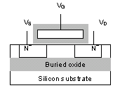
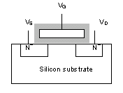
2. Silicon-On-Insulator technology Silicon-On-Insulator transistors are fabricated in a small (~100 nm) layer of silicon, located on top of a silicon dioxide layer, called buried oxide. This oxide layer provides full dielectric isolation of the transistor, and thus, most of the parasitic effects present in bulk silicon transistors are eliminated. The structure of the SOI transistor is depicted in figure 1 (a), and is very similar to the structure of the bulk transistor (figure 1 (b)). The main difference is the presence of the buried oxide.
Figure 1 (a) : SOI Transistor.
Figure 1 (b) : Bulk-Si transistor.
The presence of this buried oxide provides attractive properties to the SOI transistor. The main advantages of SOI technology are summarized below [5], [6] :
If, in addition, the silicon film is made so thin that full depletion operation is achieved [6], the following advantages are also gained:
The most attractive properties for smart card applications are: lower operating voltage without loss of speed and the enhanced security. The latter is improved in three ways. Firstly, SOI technology allows the use of more compact layouts, which makes probing more difficult. Secondly, due to the lower power and current consumption, it will be less easy to measure the variations of these quantities. Finally, SOI circuits are recognized to operate well in harsh environments especially in high temperature and radiation environments.
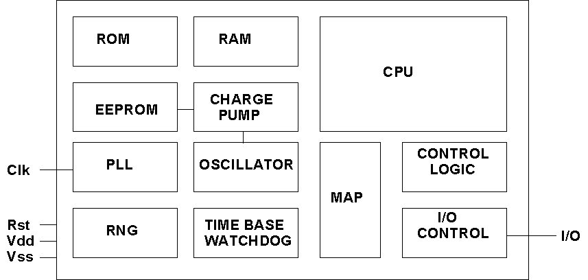
3. Chip-card circuits Based on the structure of the chip on a smart card (figure 2) [1], [7], [8], [9], we investigated the blocks already available in SOI technology and the compatibility of their performance with the smart card application.
Figure 2 : Architecture of the chip for smart applications [1], [8].
3.1 CPU Many promising results have been published about processors in SOI. A research team from Motorola has made the first very low-power low-voltage CPU-core in SOI [10]. It showed superior performances compared to similar bulk realizations. For example, at 0.9 V supply voltage, the SOI processor is twice as fast as a similar bulk processor. A test version of the Strong ARM-110 has been processed and tested by Digital Equipment [11]. It showed a performance improvement of at least 20 % over the equivalent bulk circuit, and a gain of 30 % in power dissipation. Other SOI logic circuits include Gate Arrays [12], [13] and ALUs [14]. In each case, the SOI circuits can operate faster than comparable bulk circuits, and can still operate at lower voltages. These gains in performance, and especially the low-voltage operation, are significant regarding the smart card application.
3.2 Clock generation circuits In a smart card, a clock signal is provided by the outside world and is supplied to an on-chip clock regeneration circuit, in order to stabilize the signal and to prevent clock signal manipulations. The circuit can be implemented as a Phase-Locked Loop (PLL). Such circuits have been made in SOI. For example, NTT has developed a PLL that operates at 2 V supply voltage, up to a frequency of 2 GHz [15], [16]. This shows that it is possible to conceive low-voltage clock regeneration circuits in SOI for the smart card application.
3.3 Memories Three types of memory are present on the smart card chip: ROM, RAM and non-volatile memory like EEPROM or Flash EEPROM [7]. The ROM is programmed by mask during device fabrication and no particular problem is encountered. One example of SOI realization can be found in the CPU core described above [10]. The RAM of smart cards is currently Static RAM (SRAM). The main reason is the possibility to use a power-saving mode [9]: when the CPU stays in sleep mode, the clock is fixed to the high or the low level permanently. Whereas a Dynamic RAM (DRAM) needs to be periodically refreshed, the SRAM does not need this and the presence of the supply voltage is sufficient to retain the information. A SRAM cell occupies more die area than a DRAM cell (6 transistors vs. one transistor and a tiny capacitor), but this is compensated by the absence of refresh circuit for small memories (36...256 bytes). Several manufacturers master well the fabrication of SOI-SRAM [17], [18] and SOI-DRAM [19], [20] for some years now, with speed and power performances superior to conventional bulk silicon memories. Most of the chip cards carry their user-specific information in an EEPROM or Flash EEPROM memory. Although the research in the field of the non-volatile memories in SOI is more recent, some realizations can be found. Martignone [21] described an EEPROM-based cell realized in the SOI CMOS technology of the UCL Microelectronics Laboratory. Gogl et al. realized a single-polysilicon EEPROM-cell in SOI technology for high temperature applications [22]. Two Flash EEPROM cells were described, one [23] fabricated in the UCL Microelectronics Laboratory, the other [24] fabricated by National Semiconductor.
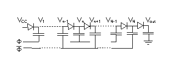
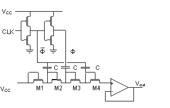
4. New circuits in SOI From the previous investigation, we identified two circuits which have never been realized in SOI : the charge pump and the random number generator. In the present work, a charge pump has been realized in the SOI-CMOS 2 µm technology of the UCL Microelectronics Laboratory. The architecture of a random number generator is also proposed. It is based on a random signal generator, realized in SOI, and some additional components to transform the random signal in a stream of random bits. These components are external discrete components in the present implementation, but could easily be integrated in SOI technology. 4.1 The charge pump Charge pump circuits, or voltage multipliers, are required to program the non-volatile memory. EEPROM or Flash EEPROM cells need a high voltage to be programmed, formerly 20 V, now towards 5 V. It can be generated on-chip from the lower supply voltage with a charge pump circuit. Most of these circuits are based on the Dickson charge pump [25], [26] (figure 3).
Figure 3 : Dickson voltage multiplier [25]. The electric charges are pumped from node to node, from the supply to the output node. The pumping is achieved by charging and discharging the capacitors, under influence of the complementary clock signals In CMOS technology, the diodes are replaced by MOS transistors, which have their gate and drain in short-circuit. The circuit we have realized is shown in figure 4.
Figure 4 : Schematic of the charge pump circuit realized in the Microelectronics Laboratory.
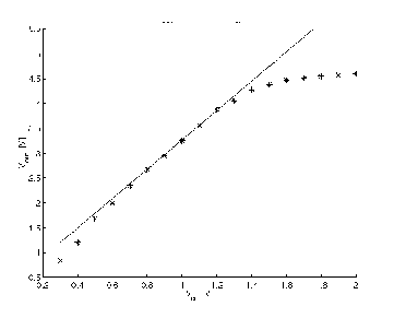
The external clock signal (CLK) is fed to the MOS diodes through two inverters, to get complementary signals. An amplifier in follower configuration has been placed at the output terminal in our test implementation in order to reduce the coupling between the load capacitance and the output voltage during the measurements. This would not be present in a practical EEPROM architecture. The experimental results are presented in figure 5 and compared to the theoretical prediction of an analytical modeling. For low supply voltages, the experimental points follow the theoretical curve fairly well. For supply voltages above 1.4 V, a saturation phenomenon can be observed. This is due to the limitation of the dynamic range of the follower-amplifier placed at the output. It can be observed that the supply voltage is multiplied by a factor of three, which was the target of our application. A programming voltage of 5 V could be obtained from a supply voltage of 1.8 V in a practical EEPROM implementation (without measurement output amplifier).
Figure 5 : Experimental (*) and theoretical (-) results for the charge pump circuit. This figure presents the output voltage Vout vs. supply voltage Vcc.
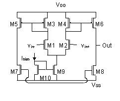
4.2 The random number generator 4.2.1 Design of the generator The random number generator in the smart card is used during the authentication procedure [9]. The terminal asks a random number to the card. The smart card encrypts it, and sends it to the terminal. If the terminal is able to decipher the number, it is authenticated by the card. Most of the generators used in current smart cards are based on deterministic algorithms expanding a random seed, thus producing " pseudo-random numbers ". But the security of the application is not necessarily guaranteed [27]. In this work we propose to develop a hardware random number generator, producing true random numbers. In the literature, very few realizations of integrated random number generators are described [28]. Some examples of random signal sources are: the frequency instability of an oscillator [28], the noise of semiconductors [29], [30], the time between two radioactive emissions [31], the number of charges in a MOS capacitor structure [32]. We use the intrinsic noise of transistors as random signal. It presents the advantage of being present in the integrated circuit itself. It is easy to use in low voltage applications. A single-stage Operational Transconductance Amplifier (OTA) is used to produce noise (fig. 6).
Figure 6 : Single-stage OTA used to produce noise.
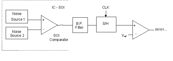
This OTA is designed to produce a high level of noise at its output. The most important contribution comes from the input differential pair M1 and M2 [33]. The noise source is integrated in a more global architecture, presented in figure 7. The experimental circuit is composed of two parts: the random signal generator, integrated in SOI, represented in the box in figure 7, and some external circuitry made up of discrete components.
Figure 7: Complete architecture of the random number generator. The random signal generator uses two independent noise sources. Their outputs provide a random signal of a few microvolts of amplitude, set around a fixed DC level. The two signals are fed into a comparator. Provided that the DC levels are the same on each comparator input, the comparator will switch randomly from one level to the other. The produced signal will be an analog random signal. The bandpass filter (B.P. filter in figure 7) selects the frequency band, and thus eliminates parasitic signals at low and high frequencies. The random analog signal is then sampled and compared to a reference value. This reference value must be the mean of the random signal. The clock signal used for the sampling determines the speed at which the random bits will be produced.
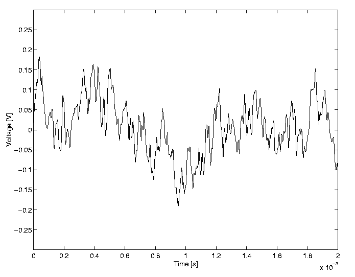
4.2.2 Experimental results The output signal of the SOI random signal generator is shown in figure 8. The random signal is modulated by a low frequency signal. The band-pass filter will eliminate the latter. Sequences of random bits were produced using this random signal in the circuit described above. Menezes et al. ( [34], Chapter 5, pp. 169-190 ) propose 5 statistical tests to check for the randomness of the sequences: the equidistribution test, the serial test, the gap test, the poker test, the runs test and the autocorrelation test. When applying the tests to the produced sequences, only 11 % of them pass the 5 tests successfully. The other sequences present a bias, that is a clear preference for "0"s or "1"s. This seems to be a general phenomenon affecting hardware random number generators [27], [34]. It is possible to de-skew the sequences by using de-skewig algorithms. Here we used Von Neumann method and the parity bit method [27]. In that case, 96 % of the produced sequences pass the 5 statistical tests. It is possible to de-skew the sequences by using de-skewig algorithms. Here we used Von Neumanns method and the parity bit method [27]. In that case, 96 % of the produced sequences pass the 5 statistical tests.
Figure 8: Output voltage of the SOI random signal generator vs. time.
5. Conclusion The objective of this work was to demonstrate the feasibility of realizing the smart card IC in Silicon-On-Insulator (SOI) technology. In the first part, we established the global architecture, and we checked in the literature which circuit blocks have already been demonstrated in SOI. For most of the circuit parts, a realization exists, and can be adapted for use in the smart card. We identified two circuit blocks, never realized in SOI up to now to our knowledge : the charge pump, and a random number generator. The charge pump has been realized and tested. A new architecture for a random number generator is proposed. A random signal generator has been processed in SOI and is used to produce random numbers. In the next version of the generator, a regulation circuit for the DC levels must be included. This will enhance the immunity to external effects (temperature, electromagnetic waves).
6. References [1] Fancher C.H., In your pocket : smart cards, in IEEE Spectrum, vol. 34, n° 2, february 1997, pp. 47-53. [2] Jarvis C.R., Beyond the Phone Card : Emerging Smart Card Opportunities, in GEC Review, pp. 131-137, vol. 12, n° 3, 1997. [3] Quisquater J.-J., The adolescence of smart cards, in Future Generation Computer Systems, n° 13, 1997, pp. 3-7. [4] http://www.dice.ucl.ac.be/~dhem/cascade [5] Colinge J.-P., Performances of Low-Voltage, Low-Power SOI CMOS Technology, in Proceedings 21st Int. Conference on Microelectronics, vol. 1, september 1997, pp. 229-235. [6] Colinge J.-P.,Silicon-on-InsulatorTechnology: Materials to VLSI, 2nd edition, Kluwer Academic Publishers, 1997. [7] Guillou L.C., Ugon M., Quisquater J.-J., The Smart Card. A standarized Security Device Dedicated to Public Cryptology, in Contemporary Cryptology, edited by Simmons G.J., IEEE Press, 1992, pp. 561-613. [8] Motorola, Technical Summary, MSC0501, 8-bit microcontroller with Modular Arithmetic Processor, 1997. [9] Rankl W., Effing W., Smartcard Handbook, Wiley, 1997. [10] Huang W.M., Papworth K., Racanelli M., John J.P., Foerrstner J., Shin H.C., Park H., Hwang B.Y., Wetteroth, Hong S., Shin H., Wilson S., Cheng S., TFSOI CMOS Technology for sub-1V Microcontroller Circuits, in IEDM, 1995, pp. 59-62. [11] Mistry K., Grula G., Sleight J., Bair L., Stephany R., Flatley R., Skerry P., A 2.0 V, 0.35 µm Partially Depleted SOI-CMOS Technology, in IEDM, 1997, pp. 583-586. [12] Kimio U. et al., A CAD-Compatible SOI/CMOS Gate Array having Body Fixed Partially Depleted Transistors, in IEEE International Solide-State Circuits Conference, 1997, pp. 288-289. [13] Masayuki et al., 0.25 um CMOS/SIMOX Gate Array LSI, in IEEE International Solide-State Circuits Conference, 1996, pp. 86-87. [14] Tsuneaki F. et al., A 0.5 V 200 MHz 1-Stage 32b ALU using a Body Bias Controlled SOI Pass-Gate Logic, in IEEE International Solide-State Circuits Conference, 1997, pp 286-287. [15] Fujishima M., Asada K., Omura. Y, Izumi K., Low Power ˝ Frequency Dividers Using 0.1 [16] Kado Y, Suzuki M., Koike K., Omura Y., Izumi K., A 1GHz/0.9 mW CMOS/SIMOX Divide-by-128/129 Dual Modulus Prescaler Using a Divide-by-2/3 Synchronous Counter, in IEEE Journal of Solide-State Circuits, vol. 28, n° 4, april 1993, pp. 513-517. [17] Kikuchi T., Onishi Y., Hashimoto T., Yoshida E., Yamaguchi H., Wada S., Tamba N., Watanbe K., Tamaki Y., Ikeda T., A 0.35 m m ECL-CMOS Process Technology on SOI for 1 ns Mega-bits SRAM’s with 40 ps Gate Array, IEDM, 1995, pp. 923-926.[18] Lu H., Yee E., Hite L., Houston T., Sheu Y.D., Rajgopal R., Shen C.C., Hwang J.M., Pollack G., A 1-M bit SRAM on SIMOX material, in Proceedings 1993 IEEE International SOI Conference, 1993, pp. 182-183. [19] Oashi T. et al., 16 Mb DRAM/SOI Technologies for Sub 1 V Operation in IEDM, 1996, pp. 609-612. [20] Koh et al., 1 Giga Bit SOI DRAM with Fully Bulk Compatible Process and Body-Contacted SOI MOSFET Structure, in IEDM, 1997, pp. 579-582. [21] Martignone R., Analog Single-Poly Floating-Gate Memories for Neural Network Applications, Travail de fin d études, Laboratoire de Microélectronique, UCL, 1996. [22] Gogl D., Burbach G., Fiedler H.-L., Verbeck M., Zimmermann C., A Single-Poly EEPROM Cell in SIMOX technology for High-Temperature Applications up to 250 °C, in IEEE Electron Device Letters, vol. 18, n°11, nov. 1997, pp. 541-543. [23] Zaleski A., Ioannou D.E., Flandre D., Colinge J.P., Design and performance of a new Flash EEPROM on SOI (SIMOX) substrates, in Proceedings 1994 IEEE International SOI Conference, oct. 1994, pp. 13-14. [24] Chi M.-H., Bergemont A., Programming and erase with floating-body for high density low voltage Flash EEPROM fabricated on SOI wafers, in Proceeding 1995 IEEE InternationalSOI Conference, oct. 1995, pp. 129-130. [25] Dickson J.F., On-Chip High Voltage Generator in NMOS Integrated Circuits Using an Improved Voltage Multiplier Technique, in IEEE Journal of Solide-State Circuits, vol. SC-11, n° 3, june 1976, pp. 374-378. [26] Witters J.S., Groeseneken G., Maes H.E., Analysis and Modeling of On-Chip High Voltage Generator Circuits for Use in EEPROM Circuits, in IEEE Journal of Solide-State Circuits, vol. 24, n° 5, october 1989, pp. 1327-1380. [27] http://ds.internic.net/rfc/rfc175 [28] Fairfield R.C., Mortenson R. L., Coulthart K.B., An LSI Random Number Generator, in Advances in Cryptology, Proceedings of CRYPTO 84, pp. 203- 230. [30] http://shell.rmi.net/~comscire [31] http://www.fourmilab.ch/hotbits [32] Agnew G.B., Random Sources for Cryptographic systems, in Advances in Cryptology, EUROCRYPT 87, pp. 77-81. [33] Dillies J., Etude, mesures, réalisation de dispositifs à haut rapport signal sur bruit en technologie SOI, Travail de fin d études, Laboratoire de Microélectronique, UCL, 1995. [34] Menezes A.J., van Oorschot P.C., Vanstone S.A., Handbook of Applied Cryptography, CRC Press, 1996.
|
|
This paper was originally published in the
Proceedings of the 1st Workshop on Smartcard Technology, May 10-11, 1999, McCormick Place South Chicago, Illinois, USA
Last changed: 18 Mar 2002 ml |
|