Owen Harrison and John Waldron
Computer Architecture Group, Trinity College Dublin, Dublin 2, Ireland.
With the introduction of the latest generation of graphics processors, which include integer and float capable processing units, there has been intensifying interest both in industry and academia to use these devices for non graphical purposes. This interest comes from the high potential processing power and memory bandwidth that these processors offer. The gap in processing power between conventional CPUs and GPUs (Graphics Processing Units) is due to the CPU being optimised for the execution of serial processes with the inclusion of large caches and complex instruction sets and decode stages. The GPU uses more of its transistor budget on execution units rather than caching and control. For applications that suit the GPU structure, those with high arithmetic intensity and parallelisability, the performance gains over conventional CPUs can be large. Another factor in the growth of interest in general purpose processing on GPUs is the provision of more uniform programming APIs by both major graphics processor vendors, Nvidia with CUDA (Compute Unified Device Architecture) [1] and AMD with CTM (Close To Metal) [2].
The main obstacle with achieving good performance on a GPU processor is to ensure that all processing units are busy executing instructions. This becomes a challenge in consideration of Nvidia's latest processor, which contains 128 execution units, given the restrictions of its SPMD (Single Program Multiple Data) programming model and the requirement to hide memory latency with a large number of threads. With respect to private key cryptography and its practical use, a challenge exists in achieving high efficiency particularly when processing modes of operation that are serial in nature. Another practical consideration is the current development overhead associated with using a GPU for cryptographic acceleration. Client applications would benefit from the ability to map their general cryptographic requirements onto GPUs in an easy manner.
In this paper we present a data model for encapsulating cryptographic functions which is suitable for use with the GPU. The application of this data model and the details of its interaction with the underlying GPU implementations are outlined. In particular we investigate how the input data can be mapped to the threading model of the GPU for modes of operation that are serial and parallel in nature. We show the performance of these modes and use our optimised AES implementation to determine the overhead associated with using a flexible data model and its mapping to the GPU. Also included in the paper is a study of the issues related to the mixing of modes of operation within a single GPU call.
Motivation: The motivation for this research is based on the GPU acting as a general guide for the long-term direction of general purpose processing. X86 architectures are bottlenecking with limited increase in clock frequency reported in recent years. This is being tackled by the addition of cores to a single die to provide growth in the total available clock cycles. The GPU is the logical extreme of this approach where the emphasis has always been on more but simpler processing elements. The upcoming AMD's Accelerated Processing Unit (Swift) [3] architecture is a reasonable compromise where a CPU and GPU are combined onto a single chip. Also Intel are developing computing solutions under the TeraScale banner which include a prototype of an 80 core processor. Using GPUs as a research platform exposes the issues that general purpose processing will encounter in future highly parallel architectures. Another motivation is the use of GPUs as a cryptographic co-processor. The types of applications that would most likely benefit are those within a server environment requiring bulk cryptographic processing, such as secure backup/restore or high bandwidth media streaming. We also wish to show the implications of the inclusion of the GPU as a generic private key cryptographic service for general application use.
Organisation: In Section 2 a brief description of the essentials in GPU hardware used is outlined, along with the CUDA programming model. Section 3 shows the related work in cryptography on non general purpose processors with a focus on GPUs. We present an implementation of AES on the Nvidia's G80 architecture and show its performance improvements over comparable CPU and GPU implementations in Section 4. In Section 5 we introduce the generic data model suited to GPUs, which is used to encapsulate application cryptographic requirements. Section 6 describes in detail the steps of mapping from the generic data structure to underlying GPU implementations. All three previous sections are combined by the implementation of modes of operation using the outlined data model and the optimised AES implementation in Section 7. This shows the overheads associated going from a hardcoded to a more general purpose implementation.
Physical View: The G80 can consist of up to 16 multiprocessors within a single chip. Each of these multiprocessors consist of 8 ALU (Arithmetic and Logic Unit) units which are controlled by a single instruction unit in a SIMD (Single Instruction Multiple Data) fashion. The instruction unit only issues a single instruction to the ALUs every four clock cycles. This creates an effective 32 SIMD width for each multiprocessor, ie. a single instruction for 32 units of data. Each multiprocessor has limited fast on-chip memory consisting of 32 bit register memory, shared memory, constant cache and texture cache. All other forms of memory, linear, texture arrays are stored in global memory, ie. off-chip. GPUs can be used in arrangements of multiple chips on a single graphics card and also multiple boards on a single mother board. For all implementations and comparisons with CPUs we have restricted the arrangements used to single GPU and single CPU core.
Execution Model: The CUDA programming model provides a way to programme the above chip in a relatively straight forward manner. The programmer can define threads which run on the G80 in parallel using standard instructions we are familiar with within the field of general purpose programming. The programmer declares the number of threads which must be run on a single multiprocessor by specifying a block size. The programmer also defines multiple blocks of threads by declaring a grid size. A grid of threads makes up a single kernel of work which can be sent to the GPU and when finished, in its entirety, is sent back to the host and made available to the CUDA application.
Two more points of note which are relevant to this paper. First, all threads within a single block will run only on a single multiprocessor. This allows threads within a single block to have the ability to share data with other threads within the block via shared memory. Inter block communication is not possible as there is no synchronisation method provided for this. Second, due to the 32 SIMD wide execution arrangement described above, Nvidia have introduced the notion of a warp. A warp represents a grouping of threads into a unit of 32. These threads run on the same multiprocessor for the entire 4 cycles required to execute a single instruction. Threads are assigned to a warp in a simple serially increasing order starting a 0 for the first thread within a block. Performance issues can arise when a group of 32 threads diverge in their code path, this causes the entire 4 cycles to be run for every unique instruction required by the 32 threads.
Harrison et al. [8] presented the first CPU competitive implementation of a block cipher on a GPU. They used the latest DX9 compliant generation of graphics processor to implement AES, namely an Nvidia 7900GT. These processors support a more flexible programming model compared to previous models, whereby certain stages of the graphics pipeline can execute C like programmer defined threads. However, the 7900GT only supports floating point operations. 3 different approaches were investigated to overcome the lack of integer bitwise operations on the programmable portion of the pipeline. The XOR operation was simulated using lookup tables for 4 bit and 8 bit XORs, and also the hardware supported XOR function within the final stage (ROP) of the pipeline. Their results showed that a multipass implementation using the built in XOR function combined with a technique called ping-ponging of texture memory to avoid excess data transfers across the PCIe bus could be used to achieve a rate of 870Mbps.
More recently the latest generation of hardware, which supports integer data types and bitwise operations, has been used by Yang et al. [9] to produce much improved performance results. This paper focuses on a bitslicing implementation of DES and AES which takes advantage of the AMD HD 2900 XT GPU's large register size. The GPU is used as a 4 way 32 bit processor which operates on four columns of 32 bitsliced AES state arrays in parallel. They show rates of 18.5Gbps processing throughput for this bitsliced AES implementation. A bitsliced implementation isn't suitable for general purpose use as it requires heavy preprocessing of the input blocks. The authors [9] argue that their bitslicing approach can be put to use as a component in template-based key searching utility or for finding missing key bytes in side channel attacks whereby the input state is static relative to the key. A conventional block based implementation of AES is also presented in this paper, running at rates of 3.5Gbps. Whether this includes transfers of input/output blocks across the PCIe bus is not indicated.
Other non general purpose processors used for private key cryptography include various ASIC designs such as [11] [12] [13] and custom FPGA efforts [14] [15]. GPUs have also been applied in the field of public key cryptography. A paper by A. Moss et al. [10] tackles the problem of executing modular exponentiation on an Nvidia 7800 GTX. They present promising results showing a speed up of 3 times when compared to a similar exponentiation implementation on a standard X86 processor. Also related to graphics processors, Costigan and Scott [16] presented an implementation of RSA using the Playstation's 3 IBM Cell processor. They were able to increase the performance of RSA using the Cell's 8 SPUs over its single PowerPC core.
As previously mentioned the G80 architecture supports integer bitwise operations and 32 bit integer data types. These new features, which are shared by all DX10 [6] compatible GPUs, simplify the implementation of AES and other block ciphers. This allows for a more conventional AES approach compared to implementations on previous generations of graphics processors. We based our implementations around both the single 1KB and 4 x 1KB precalculated lookup tables which were presented in the AES specification paper [17], see Equations 1 and 2 respectively.
As XORs are supported in the programmable section of the graphics pipeline, there is no need to use the ROP XOR support, which required multiple passes of the pipeline - one for each XOR operation. Each thread that is created, calculates its own input and output address for a single data block and runs largely in isolation of other threads in a single pass to generate its results. The simple thread to I/O data mapping scheme used for all implementations reported in this section is as follows. Each thread's index relative to the global thread environment for a kernel execution is used as the thread's offset into the input and output data buffers:
![\begin{verbatimtab}[4]
int index = threadIdx.x +
(blockIdx.x * blockDim.x);
uint4 state = pt[index];
ct[index] = state;
\end{verbatimtab}](img7.png)
where blockDim is the number of CUDA blocks within the CUDA grid, blockId is the current CUDA block the thread exists within and threadId is the current thread index within the CUDA block. As CTR is a parallel mode of operation, each thread works on a single AES block independently of other threads. To achieve high performance on a GPU or any highly multi-threaded processor, an important programming goal is to increase occupancy. The level of occupancy on a parallel processor indicates the number of threads available to the thread scheduler at any one time. High occupancy ensures good resource utilisation and also helps hide memory access latency. It is for occupancy reasons that we create a single thread for each input block of data.
A nonce is passed to all threads through constant memory and the counter is calculated in the same manner as the data offsets above. Rekeying was simplified by using a single key for all data to be encrypted, with the key schedule generated on the CPU. The reason for implementing the rekeying process on the CPU rather than the GPU is that it is serial in nature, thus the generation of a key schedule must be done within a single thread. It would be an unacceptable overhead per thread (ie. per data block) when processing a parallel mode of operation, for each thread to generate its own schedule.
Host and Device Memory: We investigated using both textures and linear global memory to store the input and output data on the device. Through experimentation we found global memory to be slightly faster than texture memory for input data reads and writes, thus all our implementation results are based on using linear global memory reads and writes for plaintext and ciphertext data. Regarding host memory (CPU side), an important factor in performance of transferring data to and from the GPU is whether one uses page locked memory or not. Page locked memory is substantially faster than non page locked memory as it can be used directly by the GPU via DMA (Direct Memory Access). The disadvantage is that systems have limited amount of page locked memory as it cannot be swapped, though this is seen normally as an essential feature for secure applications to avoid paging sensitive information to disk.
On-chip Memory: As the main performance bottleneck for a table lookup based AES approach is the speed of access to the lookup tables, we implemented both lookup table versions using all available types of on-chip memory for the G80. The types used are texture cache, constant cache and shared memory. Shared memory is shared between threads in a CUDA block and is limited to 16KB of memory per multiprocessor. It should be noted that shared memory is divided into 16 banks, where memory locations are striped across the banks in units of 32 bits. 16 parallel reads are supported if no bank conflicts occur and for those that do occur, they must be resolved serially. The constant memory cache working set is 8KB per multiprocessor and single ported, thus it only supports a single memory request at one time. Texture memory cache is used for all texture reads and is 8KB in size per multiprocessor. To investigate the the read performance characteristics of these types of memory we devised read tests to access the three types of memory in two different ways. We split the tests into random and coherent read memory access patterns, each test accessing 5 billion integers per kernel execution. Coherent access patterns were included as there are opportunities to exploit coherent reads within shared memory, ie. reads with no bank conflicts for a half warp of 16 threads.
In Table 1 we can see the average execution times measured in seconds to perform the 5 billion reads. Constant memory performs best with regard to coherent reads, though as constant memory is single ported and the lookup tables will be accessed randomly within a warp it is of little use. Shared memory out performs in the scenario of random access reads by a large margin due to its high number of ports. It should be noted that both texture and constant memory can be loaded with data before the kernel is called, however a disadvantage to shared memory is that it must be setup once per CUDA block. Shared memory is designed for use as an inter thread communication memory within the one multiprocessor and not designed for preloading of data. This is most likely an API limitation and would help reduce the setup overhead if a mechanism existed to setup shared memory once per multiprocessor before kernel execution. In an attempt to gain from the performance benefits of coherent memory reads when using shared memory we copied a single lookup table 16 times across all 16 banks to avoid memory conflicts with careful memory addressing. However it turns out that CUDA does not allow access to all 16K, even though it advertises it as such. In fact the developer only has access to slightly less than 16KB, as the first 28 bytes are reserved for system use and if over written by force causes system instability. Various optimisations were attempted to avoid bank conflicts, the fastest approach used 16 x 1KB tables save the last entry. A simple check if the last lookup entry is being sought and its direct value is used instead.
|
AES: In Table 2 we can see the maximum performance of the different AES implementations using the different types of on-chip memory. It can be seen that the 4 x 1KB table approach, Quad Table, using shared memory performs the fastest. This approach requires the four 1KB tables to be setup within shared memory for each CUDA block of threads running. This setup can be alleviated by allocating the task of a single load from global memory into shared memory to each thread within the block. For this reason our implementation uses 256 threads per block, giving the least amount of overhead to perform the setup operation. The coherent shared memory 1KB table lookup under performs due to the extra rotates which must be executed, the extra conditional check for sourcing the last table entry as described above and the additional per CUDA block memory setup costs. Previous generations of GPUs could hide the cost of state rotates via the use of swizzling (the ability to arbitrarily access vector register components) however the G80 no longer supports this feature.
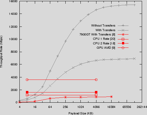
Figure 1 shows the performance of AES CTR based on the above 4 x 1KB table lookup approach. The figure exposes the requirement of many threads to hide memory read latency within the GPU. We display the throughput rate of the cipher with and without plaintext and ciphertext transfers across the PCIe bus per kernel execution. A maximum rate of 15,423Mbps was recorded without transfers and a maximum of 6,914Mbps was recorded with transfers included. We have included the rates without data transfer as we believe these to be relevant going forward where the possibility exists for either: sharing the main memory address space with the CPU, either in the form of a combined processor or a direct motherboard processor slot; or overlapping kernel execution and data transfer support on the GPU.
In the same figure we have compared our results with the latest reported AES implementations on CPUs and GPUs. Matsui [20], reports speeds of 1,583Mbps for conventional block based implementation of AES on a 2.2GHz AMD 64 processor. [18] reports an ECB AES implementation of 1,151Mbps on an AMD 64 2.4GHz 64 processor. The authors of [9], cite a speed of 3,584Mbps on an AMD HD 2900 XT GPU (AMD's DX10 compliant GPU) for their block based AES implementation, though we do not have access to the throughput rates as data sizes increase. We have included the rates achieved in [8] for AES on a GeForce 7900GT, which does provide this rate progression. With transfers included, we see a 4x speed up over the fastest CPU reported implementation and a 10x speed up without transfers. Scaling up the reported CPU AES rates to the latest available AMD core clock speed, our GPU implementation still substantially outperforms. When compared to the block based AES implementation on a GPU by [9] we can see 2x and 4x speeds ups with and without data transfers respectively.
One of the main criterion for a data model in this context is to allow the buffering of as many messages as possible that require processing into a single stream, permitting the GPU to reach its full performance potential. Exposing a payload structure to the user rather than a per message API allows the grouping of multiple messages. Also, the pressure for increase in data size can be met by providing the ability for different cryptographic functions to be combined into a single payload. Another design criteria is the use of offsets into the data for processing rather than pointers as the data will be transferred outside of the client applications memory address space rendering pointers invalid. The data model must also allow the client to describe the underlying data and keys, with key reuse, in a straight forward manner.
In the following pseudocode we can see the key data structures used. The main "payload" structure contains separate pointers for data and keys as these are normally maintained separately. A single payload descriptor structure is also referenced which is used to describe the mapping of messages to the data and key streams. The payload descriptor uses an ID to uniquely identify payloads in an asynchronous runtime environment. A high level mode for which cryptographic service is required, can be described within the payload descriptor or within the individual messages. The need for a higher level mode is due to the requirement of frameworks which abstract from multiple hardware devices having to select suitable hardware configuration to implement the entire payload. A lower level property can also be used to describe the cryptographic mode on a per message basis as can be seen in the "msgDscr" structure. The message descriptor also provides pointers for arrays of messages, IVs (Initialisation Vector), ADs (Associated Data), tags, etc. Each of these elements use the generic element descriptor which allows the description of any data unit within the data and key stream using address independent offsets. The element descriptor separates the concept of element size and count as the size of elements can sometimes indicate a functional difference in the used cipher. The return payload is the similar to the payload structure, though without the keys.
![\begin{verbatimtab}[4]
struct payload {
unsigned char *data;
unsigned char *...
...d int count;
unsigned int offset;
unsigned int size; };
\par
\end{verbatimtab}](img9.png)
Another concern when employing a data model for use with an attached processor, such as a GPU, is memory allocation for I/O buffers. For the G80 it is important to use pinned (page locked memory), this requires a request to be made to the CUDA library. The CUDA library then returns a pointer to the memory requested which can be used within the calling process. Both the input and output buffers should use pinned memory and also reuse the same buffers when possible for maximum performance. Thus there is a need for the client to be able to request both input and output buffers, to allow the tracking of its allocated buffers as the implementation cannot make a buffer reuse decision independently. This requires the encapsulating runtime, for example such as a framework like the OpenBSD Cryptoraphic Framework, to support mapping of memory allocation requests through to the library representing the hardware which will service the payload.
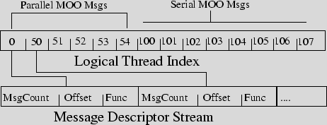
Logical Thread Index: During message serialisation a logical thread index stream is produced to facilitate the efficient location of a message ID given a thread's ID. This stream contains a single thread for each serial mode of operation (MOO) message and as many threads as there are blocks for each parallel MOO message. The entries within the logical thread index consist of only the logical thread IDs which start a message. Figure 2 shows an example of a logical thread index and how it relates to the message descriptor stream. We call the stream a logical thread index because the physical thread IDs (those assigned by the GPU), which partially determine the thread's physical location within the processor, do not necessarily map directly onto the entries within the thread index. To support balancing of work across the multiprocessors of the GPU we require the ability to assign work to different threads depending on their physical ID. Balancing work across the GPU is important for serial MOO messages, where the number of messages may be low and the size of messages may be high.
Rekeying: As outlined previously, the GPU is a highly parallel device and the key schedule generation is inherently serial, thus in general it makes most sense to implement keying on the CPU prior to payload dispatch. Our implementation uses the CPU with a hashtable cache for storing key schedules to ensure key reuse across messages. This is not just to aid efficiency at the key schedule generation stage on the CPU but also to generate the smallest key schedule stream possible. This is important for on-chip GPU caching of the key schedules. When the client application is generating the key stream for payload inclusion, it is important for the same keys to use the same position within the stream. This allows for fast optimisation of key schedule caching based on key offsets rather than key comparison.
1. Generation of the logical thread index for all messages as outlined previously. This work is carried on on the CPU.
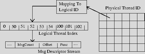
2. Mapping of the physical (GPU assigned) thread ID to a logical thread ID within each kernel thread. This was implemented using two different algorithms, one with a focus on performance and the other a focus on client application control for load balancing. The first approach maps physical to logical threads in a 1 to 1 manner in multiples of 16 x 256 threads, until the last and potentially partially full 16 x 256 group of threads. The last group of threads is allocated evenly across the multiprocessors assigning physical IDs in natural order. The reason for using 16 x 256 threads, is that the implementations used assign a fixed 256 threads per CUDA block in multiples of 16 blocks (ie. the number of multiprocessors on the 8800GTX processor). This is done to ensure the simplest form of shared memory configuration for lookup tables, see Section 4. This approach is fast to execute as a single check can eliminate the case of full thread groups where physical and logical IDs are the same. The second approach maps each physical thread into groups of 32 striped across each CUDA block. This mapping is executed for every thread and thus is slightly slower than the first approach. It however gives a more consistent mechanism for mapping physical threads to messages and thus is more controllable by the client application. In the first approach its difficult or impossible to insert serial MOO messages so that they are evenly spread across the available multiprocessors. We use the second approach in our reporting of results as it is only 0.25% slower than the first and thus the advantage out weighs the performance hit. See Section 7.3 for the effects of loadbalancing work across the GPU.
3. Search of logical thread index with logical thread ID to determine message ID for kernel. This step also calculates logical thread ID offset from beginning of message. Due to storing a digested form of the logical thread IDs, in which each entry in the logical thread index is the thread ID start of a message, the search is implemented as a binary search. A direct lookup table could be used for better performance however this would require a lookup table equal to the number of logical threads. For parallel MOO messages this would be too high an overhead in terms of data transfer and cacheability of the index. The digest version only stores a thread index entry per message within the payload and also provides an easy way to calculate the thread offset from the start thread (ie. first block) for parallel MOOs messages.
4. Use of message ID to offset into the message descriptor stream, which is used to retrieve the input data offset and other message settings.
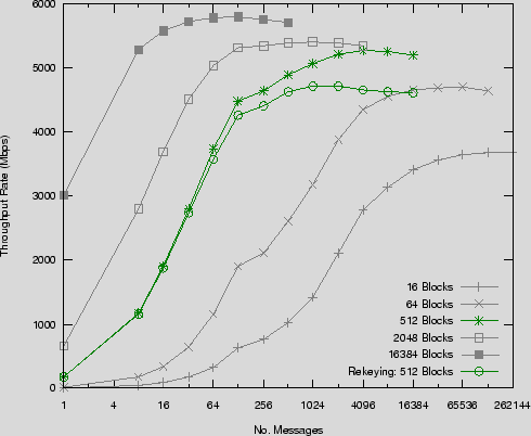
All results are based on multiple executions of a single payload with the reuse of memory buffers both for host and on device storage. This simulates the scenario of an application managing its own host memory allocations as described in Section 5. Our implementations also reuse the same key, simulating all messages being within a single cryptographic session. We also include in Figure 4 throughput rates for maximum rate rekeying, whereby each message contains its own unique key. We have highlighted the comparison of rates with and without rekeying for payloads with a message size of 512 blocks. As expected, an increasing message count results in an increasing overhead on total throughput.
The maximum throughput achieved for a parallel MOO under the generic data model was 5,810Mbps. An important observation from these figures is that we can see there is an overhead associated with using the described generic data model for abstracting the underlying implementation details. When using large messages (16384 blocks) this overhead is 16%, with medium sized messages (512 blocks) the overhead is 22% and in the worst case when using small messages (16 blocks) the overhead is 45%. The reasons for the increase in overhead as the message count increases relative to the work done, is due mainly to the caching behaviour of the index stream descriptors used on the small 8KB GPU texture caches. For example, regarding the logical thread index stream when used for a parallel MOO payload, even though it efficiently encodes one logical thread per message (the starting block) and extrapolates the remaining threads for the message, each additional message requires an extra 32 bits. We see a consistent drop off in performance for larger message counts as each binary search performed to map the physical thread ID to message ID must increasingly access global memory. There is also an increased overhead associated with CPU preprocessing of messages and the number of steps involved in the thread to message mapping process. Future work involves attempts to optimise the streams used, even though we are somewhat restricted given that the GPU is an SPMD device and fat kernels add register pressure and reduce occupancy. In particular executing parallel messages in groups of data for large payloads in small message configurations could reduce the overhead of thread to message mapping.
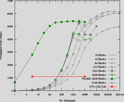
Figure 5 shows the performance rates for a serial MOO using different sizes of messages. All results are based on the CBC MOO in encrypt mode, other serial MOOs using the same block cipher performed equivalently with regards to bulk throughput rates. All messages within a single payload were of the same size, see Section 7.3 for detail on mixing sizes of messages within a payload. We have included in the figure a CPU based implementation of the OFB MOO from [18], as a point of comparison. We have also included the results for a parallel MOO for a payload with a message size of 2048 blocks from Figure 4. The figure highlights its comparison with the corresponding serial MOO message size. We can see the penalty paid for a low number of serial messages within the payload as it takes quite a number of messages before throughput substantially increases. This is easy to see in the comparison of the parallel MOO which starts at quite a reasonable throughput rate from a low message count. We can also see that there is performance to be gained by grouping blocks into threads which reduce the per message overheads discussed above, this accounts for the higher performance of the large message count serial payloads over parallel payloads. These serial results cannot be compared with the AES optimised implementation in Section 4 directly for framework overhead calculations as the optimised AES implementation is implicitly parallel.
A disturbing trend can be observed for larger serial MOO message sizes - as the number of messages increase a performance bottleneck is hit. This may be explained by the memory access pattern created by such executions. Neighbouring threads within a CUDA warp use increasingly disparate memory address locations for their input and output data as the message size increases. We have isolated this behaviour with a separate memory test in which each thread performs a series of sequential reads from global memory starting at an offset from the previous neighbouring thread equal to the number of sequential reads performed. Figure 6 presents these results for different offsets and corresponding sequential reads in increments of blocks (taken to be 16 bytes for this test). For block counts of 128 and over the memory read performance drops dramatically as the the number of active threads increase. There is not enough publicly available detail on the G80 to definitively explain this behaviour, however it is possibly a combination of level 2 cache bottleneck and a limit on the number of separate DRAM open pages supported by the DRAM controllers. Either could cause performance drops as concurrent memory reads reduce their coherency.
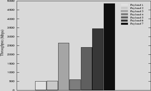
To allow the client application sufficient control over the positioning of serial MOO messages on the hardware, we have used the physical thread to message mapping described in Section 6. This allows the client to simply group all serial messages at the start of the payload if possible. The striping mapping scheme used will automatically group the messages into groups of 32 and distribute the groups evenly across CUDA blocks, which will be assigned evenly to the available multiprocessors by the CUDA library. Also, the order in which the serial messages appear in the input stream is preserved, so if the client orders messages according to their size these are maintained in their optimal ordering for SIMD work load balancing. We developed a series of tests which allows us to demonstrate the effect of different mixing configurations of serial MOO messages across a payload. Figure 7 shows the throughput rates of different payload configurations. Each payload configuration consisted of the same messages, only the ordering of the messages were changed. The absolute throughput rates are not relevant as the messages used were manufactured to fit the test requirements and not for performance. The relative difference between the scenarios clearly shows the importance of correct ordering of messages when mixing serial and parallel MOO messages within a single payload.
All payloads used 960 512-block parallel MOO messages, 992 32-block parallel MOO messages and 1024 serial MOO messages with 8 variations in message size ranging from 16 to 2048 blocks. Here is a description of each of the payload configurations used in Figure 7.
Payload 1: One serial MOO message per group of 32 threads, attempting to assign all serial MOO messages to a single multiprocessor. This assignment is not entirely possible as CUDA blocks are assigned to available multiprocessors and is beyond the control of the developer.
Payload 2: One serial MOO message per 32 threads spread evenly across the multiprocessors.
Payload 3: All serial MOO messages assigned to the minimum number of CUDA blocks. This scenario is much faster than 1 and 2 as all SIMD slots within 32 threads are occupied, even though not all multiprocessors are occupied with work.
Payload 4: A random distribution of serial MOO messages across the payload.
Payload 5: A random distribution of serial MOO messages across the payload, however grouped into 32 threads to ensure full SIMD slot usage.
Payload 6: All serial MOO messages grouped into 32 threads and spread evenly across all multiprocessors.
Payload 7: Same as Payload 6 however all serial MOO messages appear within the payload in order of their message size. All other payload configurations use a random ordering of message sizes.
From the results one can see the main priorities for client ordering of serial MOO messages within a payload are: their grouping within the device's SIMD width to ensure the SIMD slots are occupied; the even spread of serial MOO message groups across the available mulitprocessors; and the ordering of serial MOO messages according to their size to keep similar message sizes within the one SIMD grouping. A separate and notable concern when mixing function types within a payload is that the underlying implementation can suffer from increased resource pressure. The G80, like other SPMD devices only support a single code path which execute on all threads, thus the combination of function support within a single kernel via conditional blocks can increase register pressure and also increase overhead for the execution of such conditions.
In this paper we have presented an AES implementation using CTR mode of operation on an Nvidia G80 GPU, which when including data transfer rates shows a 4x speed up over a comparable CPU implementation and a 2x speed up over a comparable GPU implementation. With transfer rates across the PCIe bus not included this ratios increase to 10x and 4x respectively. We have also investigated the use of the GPU for serving as a general purpose private key cryptographic processor. The investigation covers the details of a suitable general purpose data structure for representing client requests and how this data structure can be mapped to underlying GPU implementations. Also covered are the implementation and analysis of both major types of encryption modes of operation, serial and parallel. The paper shows the issues and potentially client preventable caveats when mixing these modes of operation within a single kernel execution.
We show that the use of a generic data structure results in an overhead ranging from 16% to 45%. The main reason for the drop in performance is due to the descriptor data streams becoming too large to fit in the small texture working cache size of the G80. This per thread overhead occurs most acutely within the implementation of parallel MOO payloads with small messages and a high message count. It could be argued that in such a case a client would be better implementing a hardcoded approach if the input data structures are known in advance.
Overall we can see that the GPU is suitable for bulk data encryption and can also be employed in a general manner while still maintaining its performance in many circumstances for both parallel and serial modes of operation messages. Even given the overheads of using a generic data structure for the GPU, the performance is still significantly higher than competing implementations assuming chip occupancy can be maintained. However when small payloads are used the GPUs performance under performs both in the general and hardcoded implementations due to the resource underutilisation and the transfer overheads associated with movement of data across the PCIe bus. Further work is required in optimising the mapping of a generic input data structure to threads to improve the noted overheads. Also investigation of authenticated encryption modes of operation should be included in a similar study.